


![]()

![]()
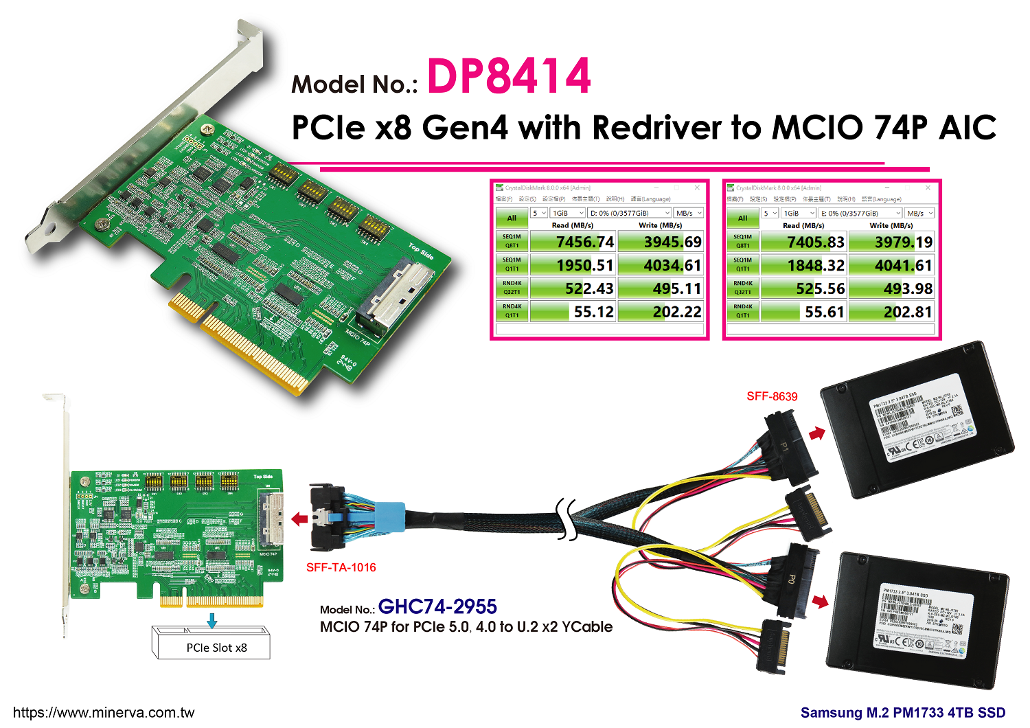
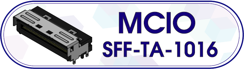
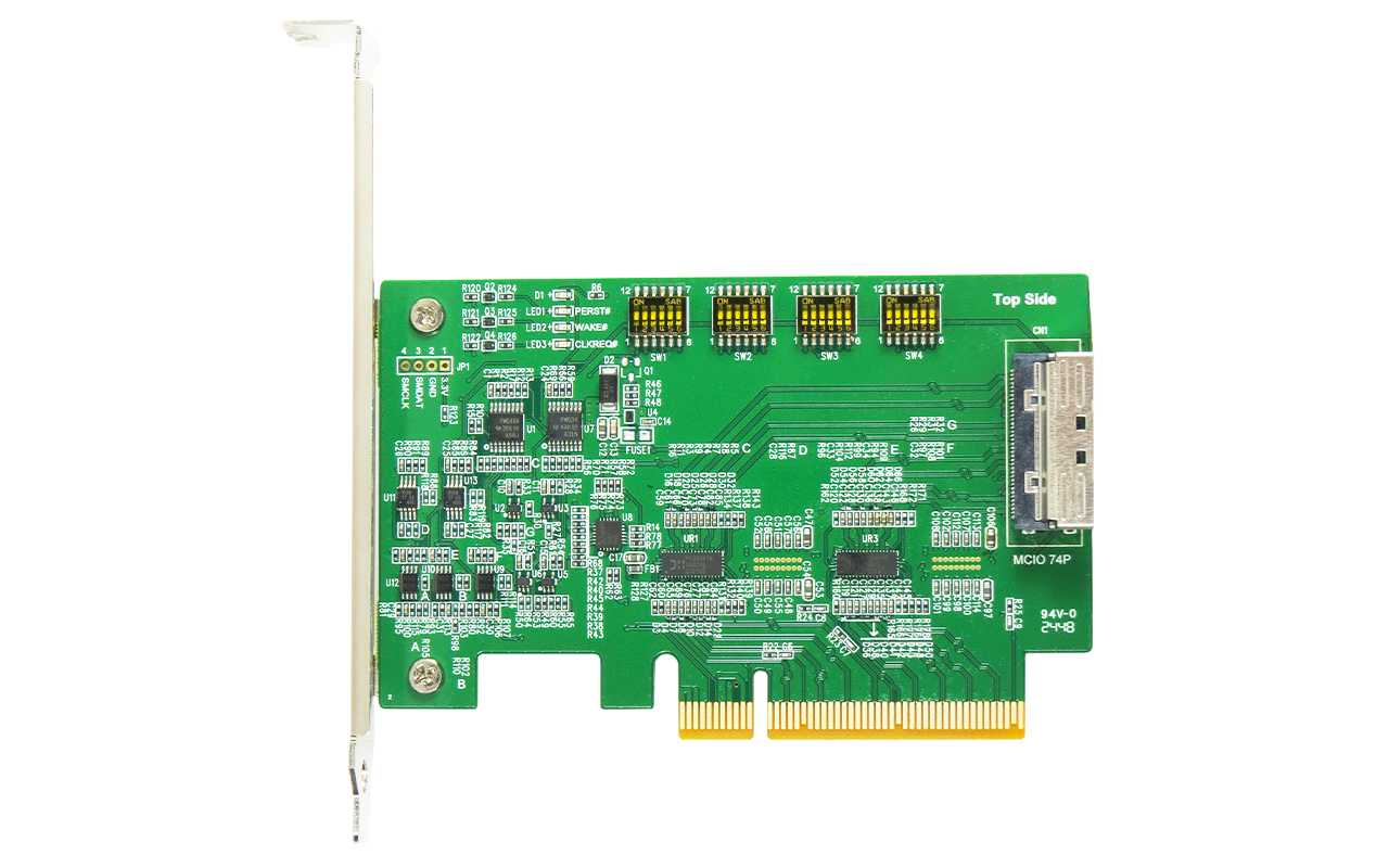
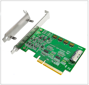
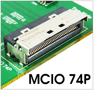
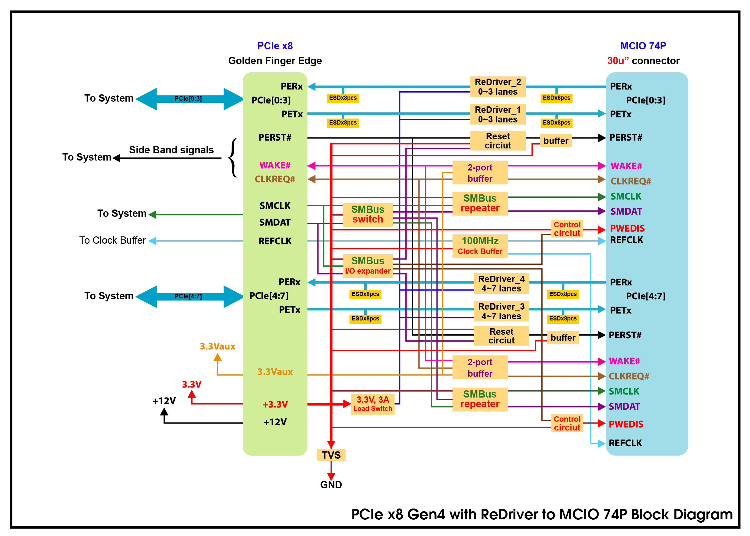
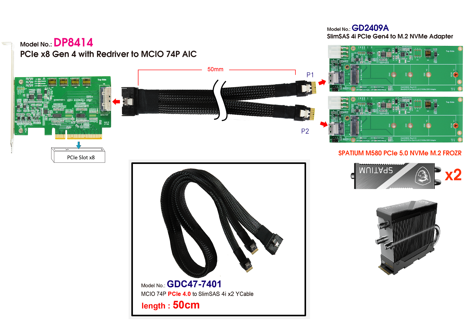
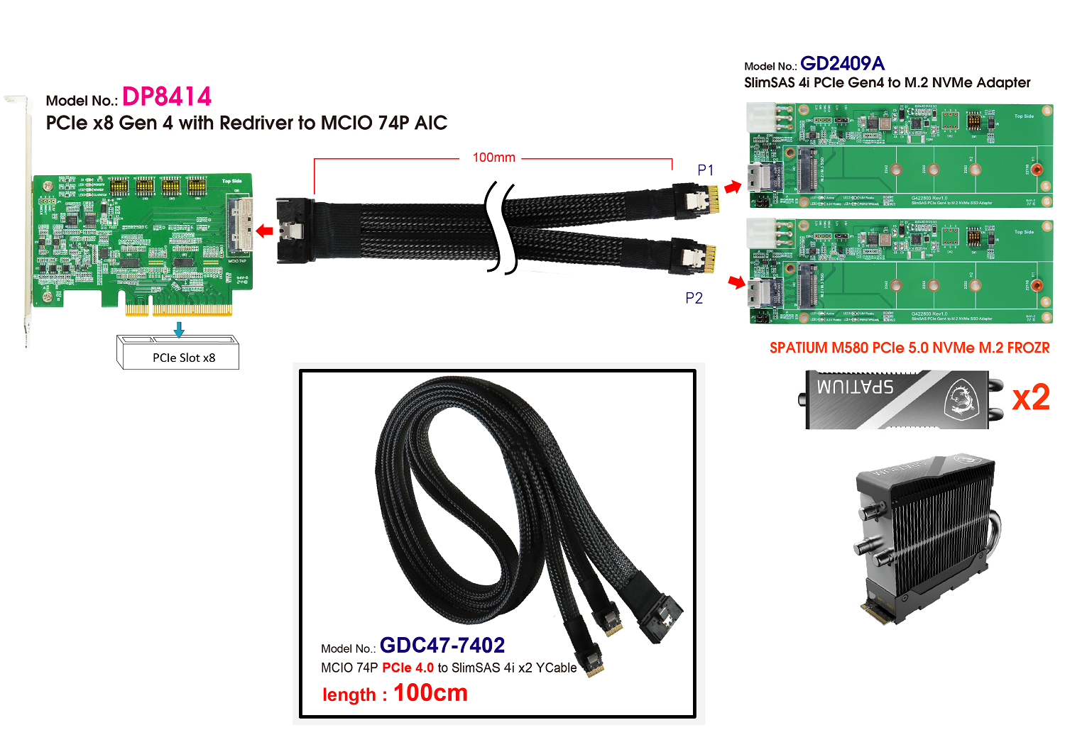
- MCIO 74P to PCIe x8 Gen4 convert
- Built-in MCIO 74P connector, 30u”connector
- Input power 3.3V with TVS and Load Switch protection to protect ReDriver controller
- PCIe 4.0 eight-lane signals input and output with ESD protection
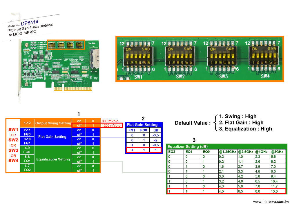
- Built-in ReDriver controller to extend PCIe 4.0, 16GT/s differential pair signals 8 lanes data link width,and may provides programmable linear equalization, output swing and flat gain.
- The PCIe 8 lanes can be bifurcated into two x4 link width to support different system topologies
- Built-in PCIe 100MHz clock buffer(Address: 0x6C) for MCIO 74P to drive longer cable length. It maybe buffered and fanned out to the MCIO 74P clock pin dual port output.
- Built-in SMBus Switch(Address: 0x70) with Reset funtion for MCIO 74P dual port SMBus communication
- Built- in SMBus bidirectional buffer repeater
- Built-in SMBus I/O Expander(Address: 0x20) for OOB(out of band) management to remote MCIO 74P Reset signals
- Built-in PERST# Bus Buffer Gate to be used over longer trace lengths and over longer cable length.
- Supports PCIe PERST# for OOB(out of band) management to remote MCIO 74P Reset
- Built-in WAKE# Bus Buffer Gate to be used over longer trace lengths and over longer cable lengths.
- Built-in CLKREQ# Bus Buffer Gate to be used over longer trace lengths and over longer cable length.
- D1 Green LED on indicates AIC ready
- LED1 Green OFF indicates PERST# Normal (Function intentionally inverted)
- LED2 Green OFF indicates WAKE# Normal (Function intentionally inverted)
- LED3 Green OFF indicates CLKREQ# Normal (Function intentionally inverted)
![]()