


![]()

Datasheet
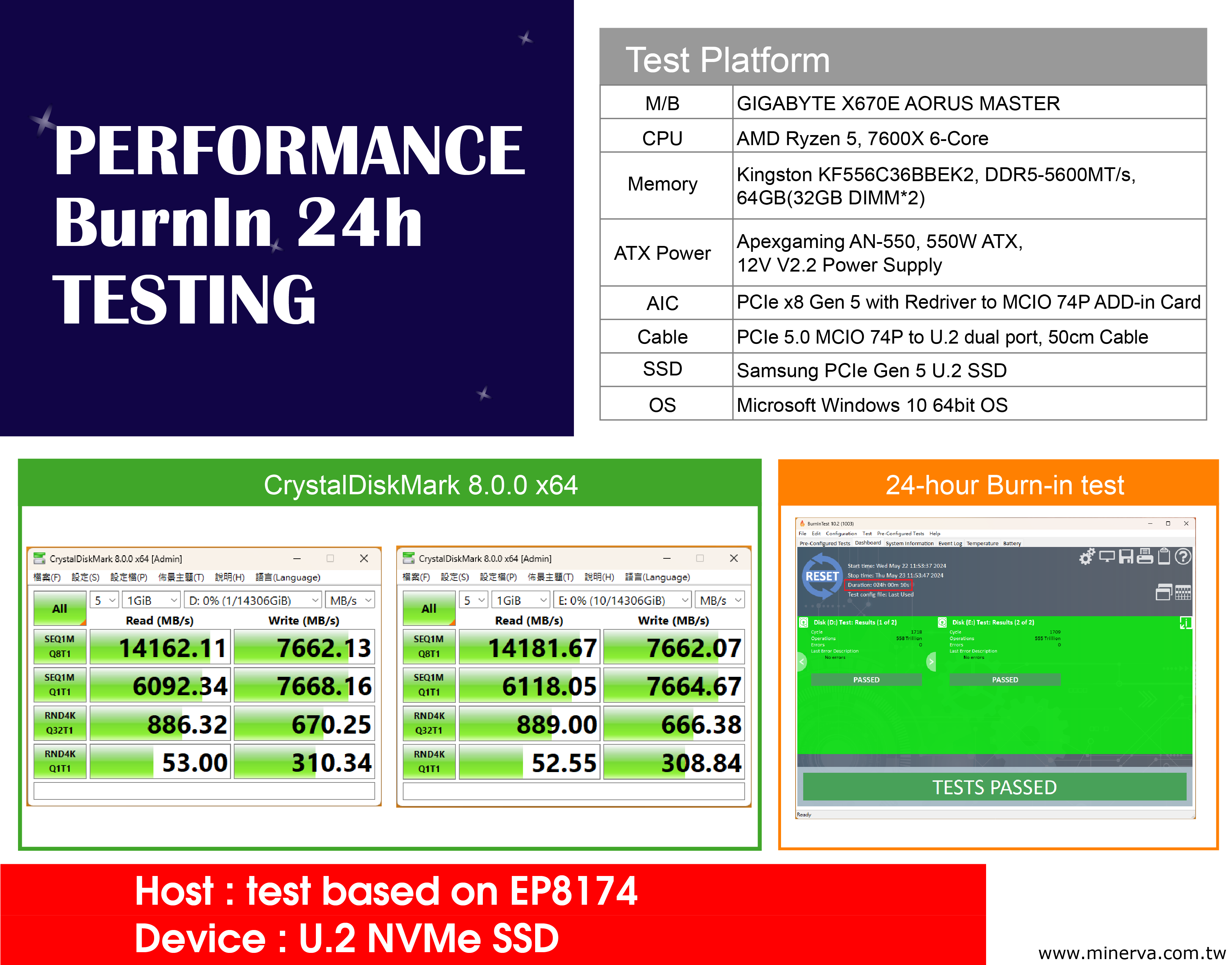
Test Report
2D drawing
![]()
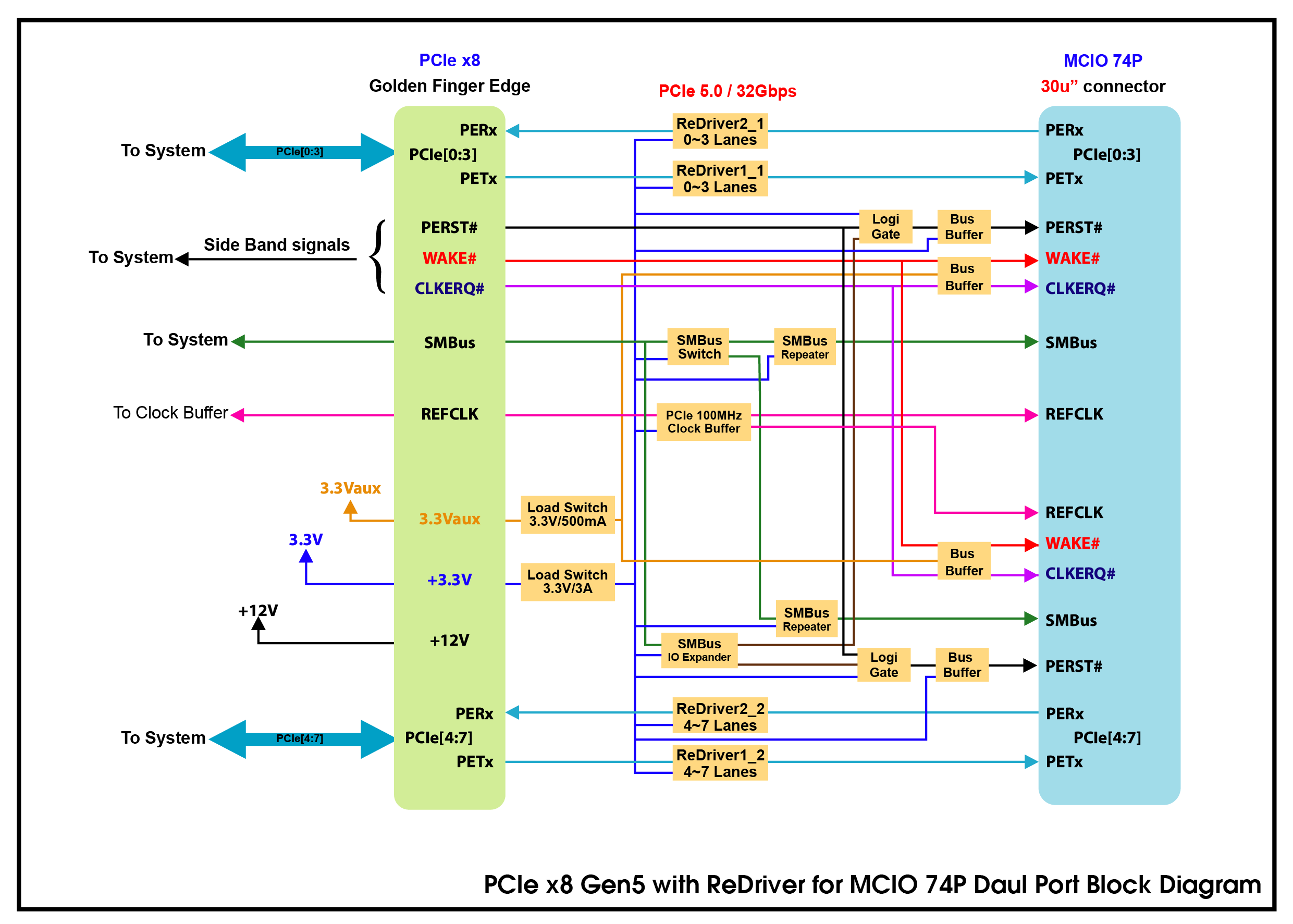
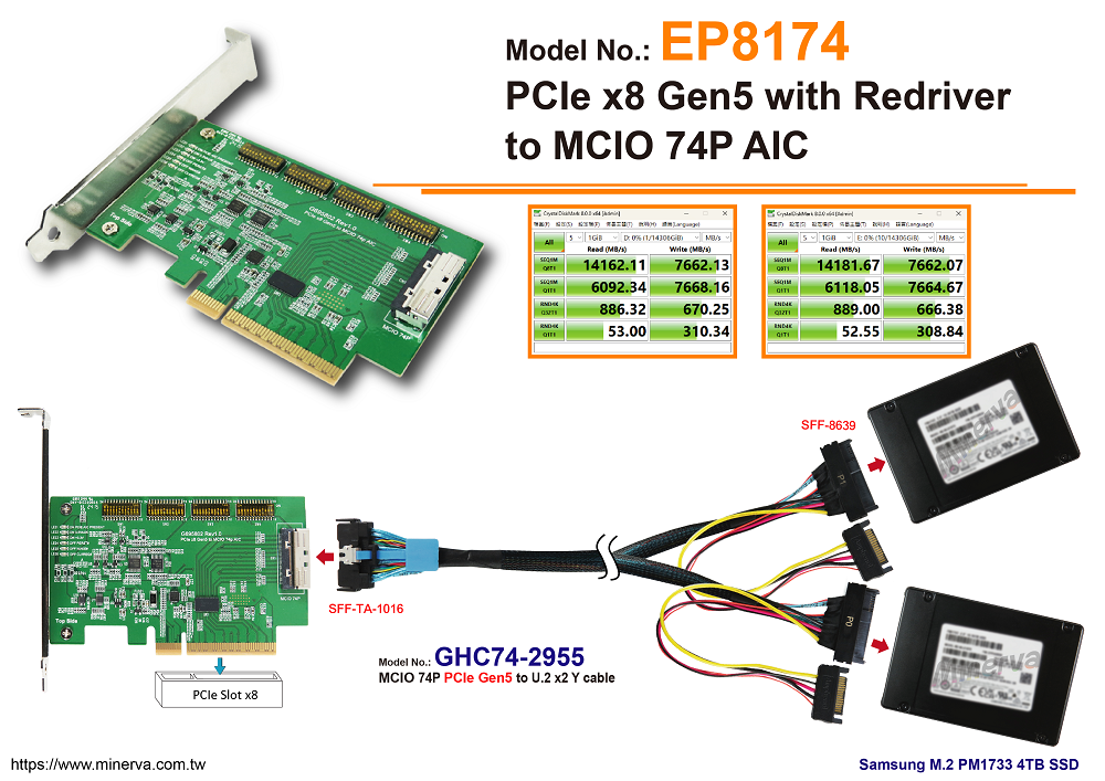
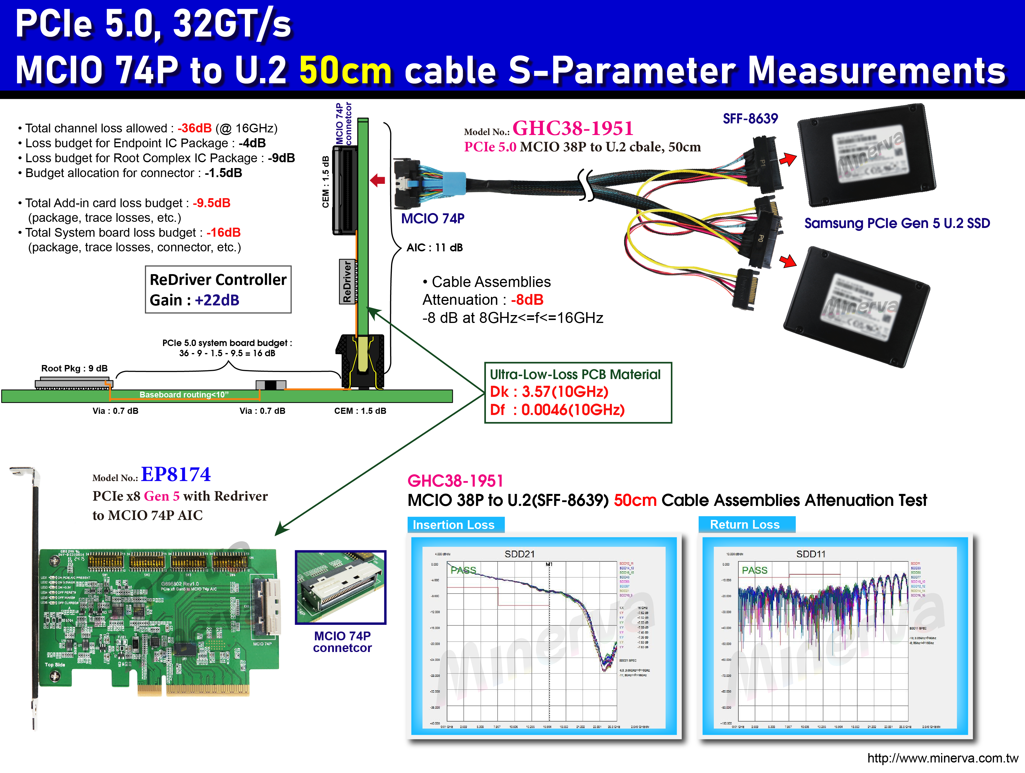
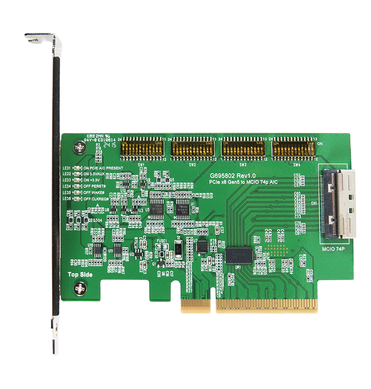
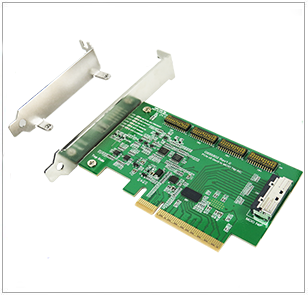
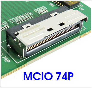
- MCIO 74P to PCIe x8 Gen5 convert
- Built-in MCIO 74P connector with 30u”(0.38um) min Au mating area plating
- Input PCIe CEM power +3.3V with Load Switch protection for ReDriver controller, SMBus switch and SMBus expander
- Input PCIe CEM power 3.3Vaux with Load Switch protection for Bus Buffer IC.
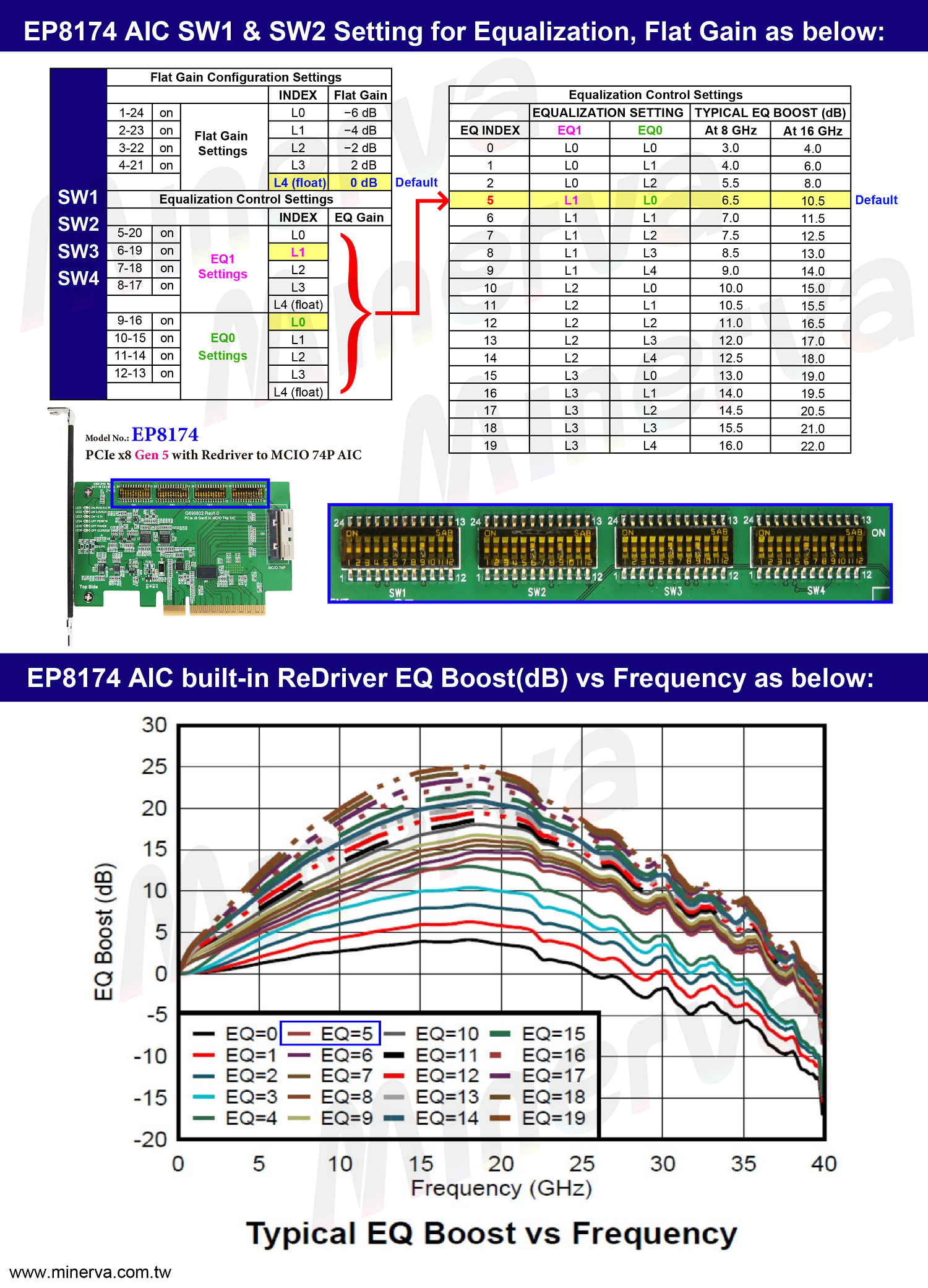
- Built-in ReDriver controller to extend PCIe 5.0, 32GT/s 8 lanes signals and may provides programmable linear equalization, flat gain.
- CTLE boosts up to 22 dB at 16 GHz
- The PCIe 8 lanes can be bifurcated into two x4 link width to support different system topologies
- Built-in PCIe 100MHz clock buffer(Address: 0x6C) for MCIO 74P to drive PCB more trace reach and longer cable length.
- Built-in SMBus Switch(Address: 0x70) with Reset funtion for MCIO 74P SMBus communication
- Built-in SMBus I/O Expander(Address: 0x20) for OOB(out of band) management to remote MCIO 74P Reset signals
- Built-in PERST# Bus Buffer Gate to be used in PCB more trace reach and longer cable length.
- Supports PCIe PERST# for OOB(out of band) management to remote MCIO 74P Reset signals.
- Built-in WAKE# Bus Buffer Gate to be used in PCB more trace reach and longer cable length.
- Built-in CLKREQ# Bus Buffer Gate to be used in PCB more trace reach and longer cable length.
- LED1 Green ON indicates AIC ready
- LED2 Green ON indicates 3.3Vaux ready
- LED3 Green ON indicates +3.3V ready
- LED4 Green OFF indicates PERST# Normal (Function intentionally inverted)
- LED5 Green OFF indicates WAKE# Normal (Function intentionally inverted)
- LED6 Green OFF indicates CLKREQ# Normal (Function intentionally inverted)