


![]()

Datasheet
GHC38-1951 Test Report
GHC38-1952 Test Report
GHC38-1951+GE0146A Test Report
GHC38-1952+GE0146A Test Report
2D drawing
![]()
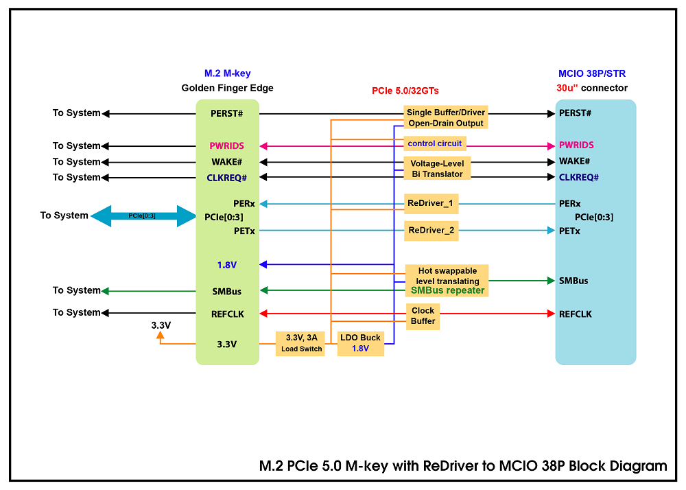
- Built- in 3.3V, 3A Load Switch with Reverse Current Protection and Controlled Turn-On
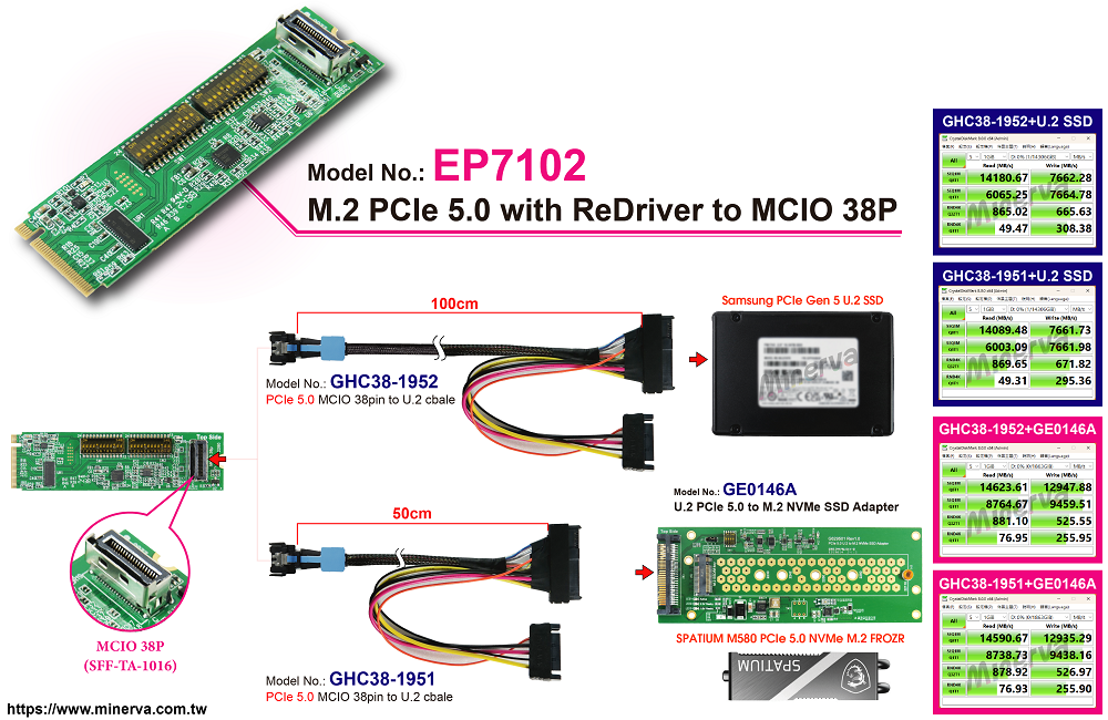
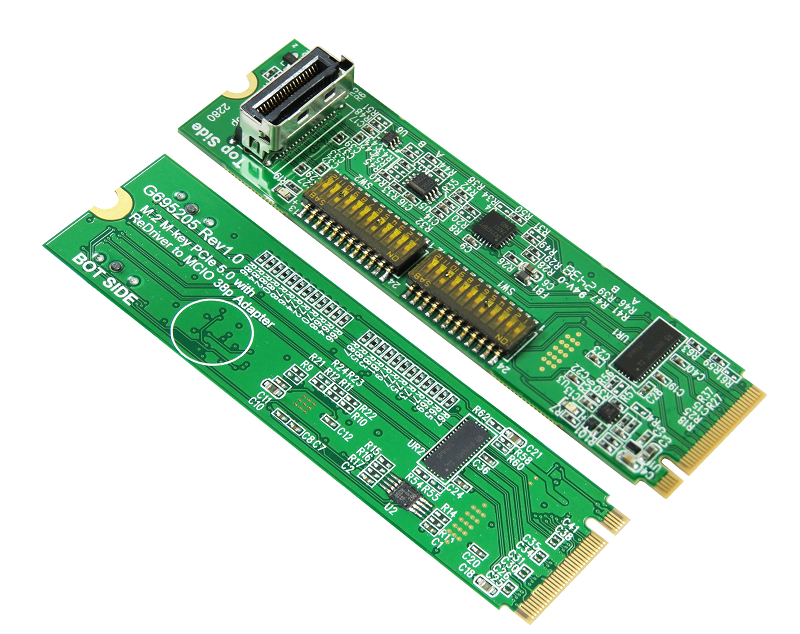
- MCIO 38P (SFF-TA-1016) to M.2 PCIe 5.0 convert
- Built- in MCIO 38P connector with 30u”(0.76um) min Au mating area plating
- Built- in PCIe ReDriver to extend PCIe 5.0, 32GT/s differential pair signals
- Built- in PCIe 100MHz Clock buffer to drive longer trace lengths and longer cable
- ◆ The REFCLKp signal, it is tied to MCIO 38P B11 pin
- ◆ The REFCLKn signal, it is tied to MCIO 38P B12 pin
- Built- in SMBus repeater and Voltage level shift with Hot swappable level translating
- ◆ The SMCLK signal, it is tied to MCIO 38P A8 pin
- ◆ The SMDAT signal, it is tied to MCIO 38P A9 pin
- Built- in PERST# Bidirectional Voltage-Level Translator, it is tied to MCIO 38P A11 pin
- The WAKE# signal, it is tied to MCIO 38P B8 pin
- The CLKREQ# signal, it is tied to MCIO 38P A12 pin
- The PWRDIS signal signal, it is tied to MCIO 38P B9 pin
- LED1 Green ON indicates 3.3V ready
- LED2 Red from ON to OFF indicates PERST# signals normal