


![]()

Datasheet
Test report for GDC36-9201
Test report for GDC36-9202
2D drawing
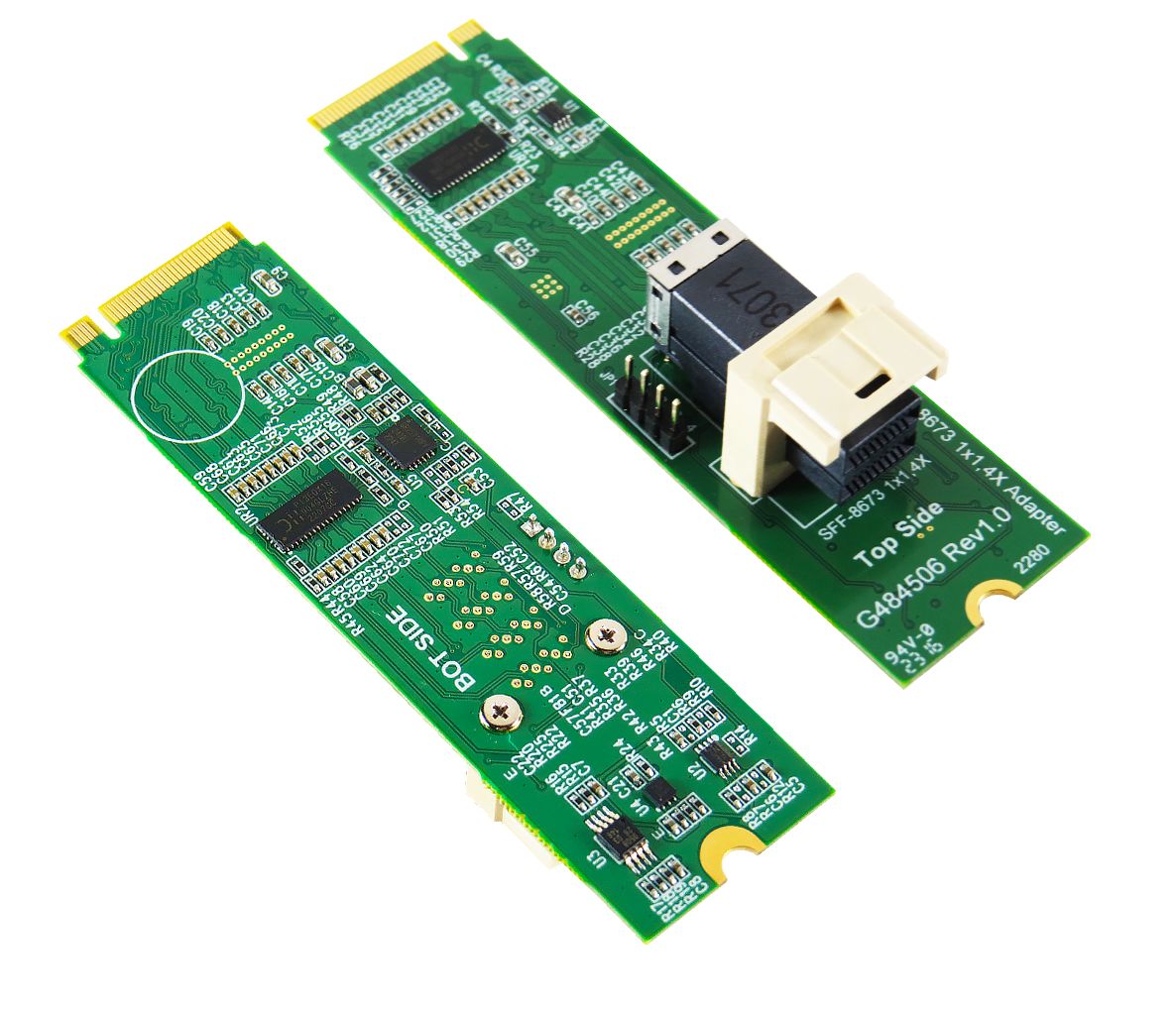
- SFF-8673 1x1, 4X to M.2 PCIe 4.0 convert
- Built- in SFF-8673 connector with 30u”(0.76um) min Au mating area plating
- Built- in PCIe ReDriver to extend PCIe 4.0, 16GT/s differential pair signals
- Built- in PCIe 100MHz Clock buffer to drive longer trace lengths and longer cable
- Built- in SMBus repeater and Voltage level shift with Hot swappable level translating
- Built- in PERST# Bidirectional Voltage-Level Translator, it is tied to SFF-8673 1x1, 4X B1 pin
- Built- in WAKE# Bidirectional Voltage-Level Translator, it is tied to SFF-8673 1x1, 4X C1 pin
- Built- in CLKREQ# Bidirectional Voltage-Level Translator, it is tied to SFF-8673 1x1, 4X B2 pin
- Built- in PWRDIS Bidirectional Voltage-Level Translator, it is tied to SFF-8673 1x1, 4X C2 pin
![]()
![]()